
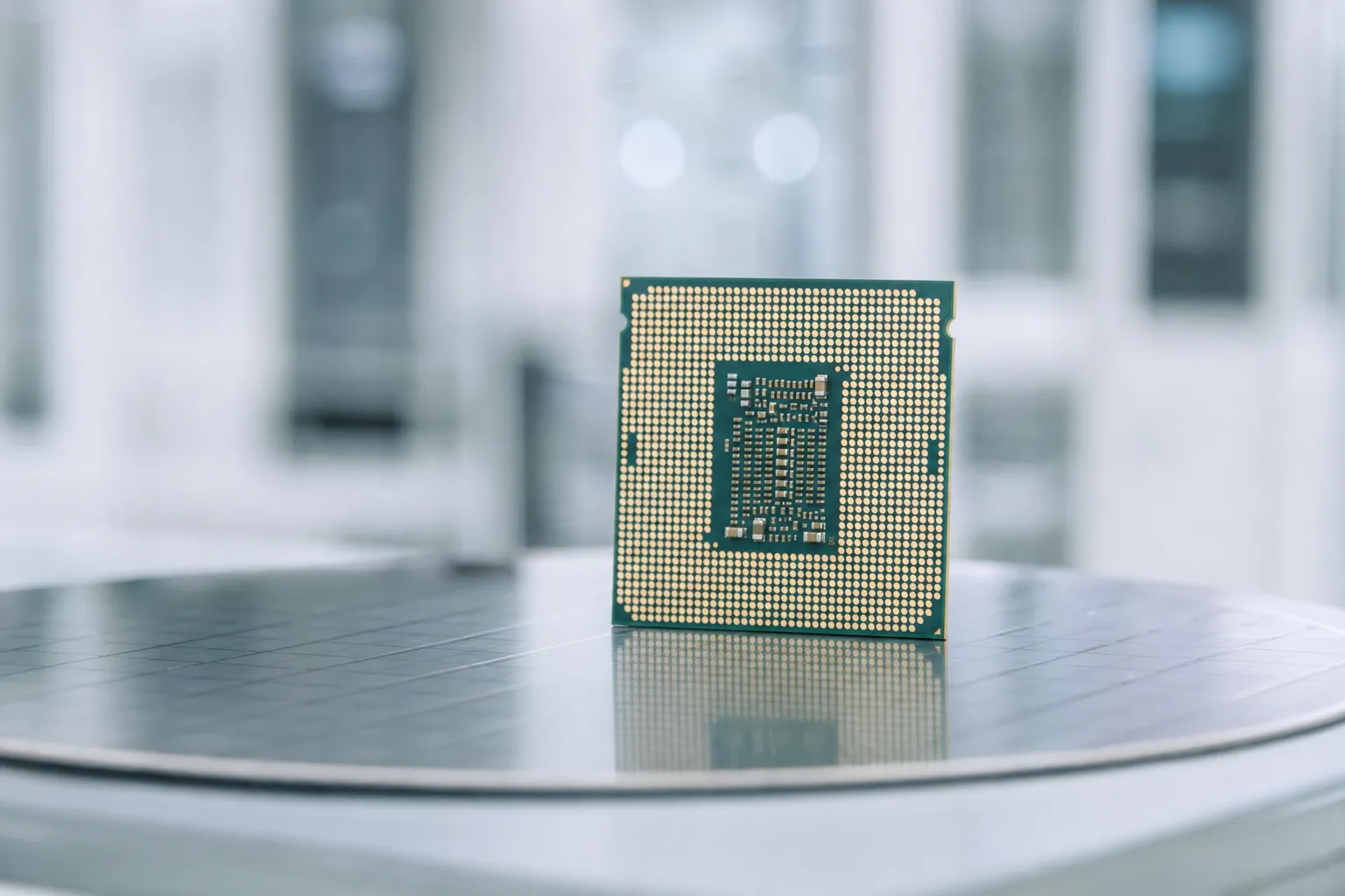
Semiconductor fabs face a widening technical challenge: advanced chip production has grown so complex that traditional process validation methods cannot keep pace with demand. Engineers must now predict how material interactions will behave under new process steps, map defects back to root causes, and validate changes before committing wafers to production—all while shrinking margins for error. AI is stepping into this bottleneck. Machine learning models can analyze vast datasets from equipment sensors, metrology tools, and defect inspection systems to identify failure patterns faster than manual analysis. This matters directly to infrastructure: as NVIDIA's GPU designs push into smaller geometries and higher transistor density, fabs building Blackwell and next-generation architectures need these predictive tools to maintain yield and throughput.
The practical implementation centers on reducing time-to-insight. Traditionally, correlating a defect signature to a process parameter required weeks of statistical analysis and repeat experiments. AI-driven systems compress this workflow by recognizing patterns across thousands of wafer lots simultaneously. Major foundries including TSMC and Samsung have begun integrating machine learning into their advanced node fabs, though specific yield improvements and detection time reductions remain largely proprietary. What is clear: as node complexity increases—particularly for 3nm and below—the computational burden of process control itself becomes a manufacturing bottleneck that only AI-scale analytics can address efficiently.
However, significant limitations persist. AI models require massive historical datasets to train effectively, which means bleeding-edge processes often lack sufficient data for robust predictions. Models trained on one fab's equipment may not transfer to another manufacturer's setup without substantial retraining. Additionally, AI excels at pattern recognition but struggles with novel failure modes that have no historical precedent—the exact scenarios that arise in first-pass yields of revolutionary architectures. The industry remains in an early adoption phase where AI augments rather than replaces process engineers, and skepticism about over-reliance on black-box predictions continues to temper deployment speed.
The infrastructure implications extend beyond individual fabs. As NVIDIA, AMD, and custom chip designers demand higher volumes of advanced silicon, the manufacturing supply chain's ability to scale depends on tools that can compress process development cycles. AI-assisted defect analysis and process optimization represent essential infrastructure for meeting the data center compute buildout that large language model training and agentic AI applications require. For NVIDIA specifically, faster fab turnaround directly translates to shorter lead times between architecture iterations and production ramp, a competitive advantage in the rapidly evolving GPU market where Blackwell and successor architectures drive revenue growth.