
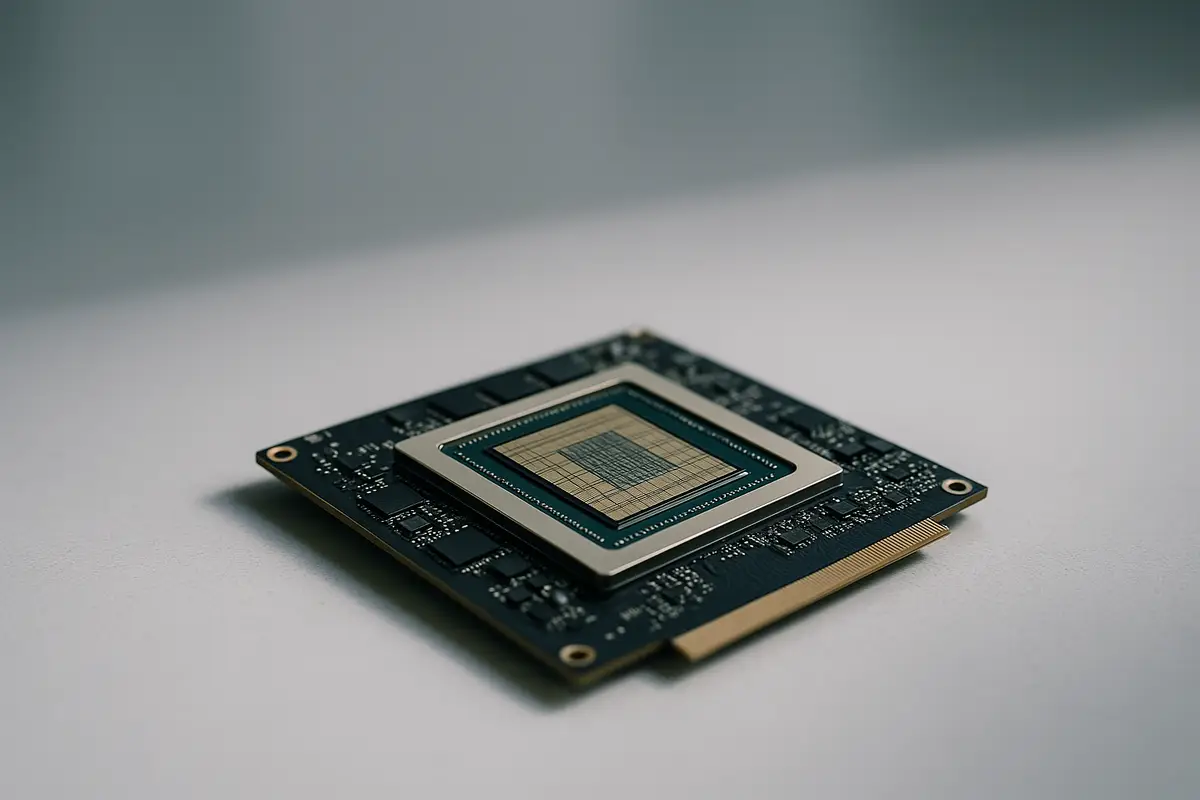
NVIDIA's fortress in AI infrastructure extends far beyond architectural innovation or manufacturing scale. According to insider reporting on the company's validation engineering practice, NVIDIA employs specialized teams tasked with exhaustive pre-launch scrutiny of every chip generation—a resource-intensive discipline that directly impacts customer trust and deployment timelines. Validation engineers at NVIDIA function as systematic fault-finders, stress-testing silicon under extreme thermal, electrical, and workload conditions before commercial availability. This process typically spans 18-24 months from tape-out to production readiness, with teams identifying and engineering fixes for issues that might otherwise surface in customer data centers at catastrophic scale. The competitive calculus is stark: a major undetected flaw in GPU memory controllers or thermal management can disable thousands of nodes across a hyperscaler's infrastructure, generating costs that dwarf NVIDIA's own validation budgets. AMD's Instinct processors and custom silicon efforts by cloud providers have periodically suffered from abbreviated validation cycles, resulting in firmware patches, performance throttling, or partial fleet quarantines—each incident reinforcing customer preference for NVIDIA's proven reliability track record.
The stakes of validation rigor became visible during the Blackwell architecture transition, where NVIDIA's validation teams identified and resolved critical thermal and power delivery issues before the GPU reached volume production. Industry sources suggest NVIDIA maintains validation teams numbering in the hundreds across multiple global facilities, with redundant testing workflows that independently verify silicon behavior across dozens of use case simulations before green-lighting manufacturing. This infrastructure investment creates a structural moat that pure architectural talent cannot replicate; competitors must either match this validation expense or accept elevated field failure rates—a calculus that forces long-term capital allocation decisions. Hyperscaler procurement teams increasingly cite validation rigor as a primary evaluation criterion, effectively penalizing entrants with unproven reliability profiles. The 2022-2023 period saw multiple instances of GPU supply chain disruption where NVIDIA's reputation for pre-validated silicon insulated it from customer defection, while competitors faced extended qualification cycles and stricter terms.
This validation advantage operates largely invisible to public markets, overshadowed by discussions of chip architecture, memory bandwidth, and CUDA ecosystem lock-in. Yet conversations with data center operators and AI infrastructure teams reveal a consensus: hardware validation speed and comprehensiveness directly impact deployment velocity and total cost of ownership. NVIDIA's ability to move from silicon discovery through customer qualification to volume production faster than competitors—while maintaining zero-defect targets—compounds over successive product generations. As NVIDIA transitions to Blackwell and successor architectures, the company's validation infrastructure must scale proportionally, supporting simultaneous certification across consumer, data center, automotive, and research compute segments. AMD, Intel, and emerging competitors must choose between matching this validation investment—requiring sustained R&D spending of $1-2 billion annually with uncertain ROI—or accepting longer time-to-market and elevated customer skepticism. For investors and industry observers, NVIDIA's validation advantage represents a less visible but more durable competitive moat than manufacturing partnerships or software ecosystems alone.